If the boards in a system are connected to each other on the CT bus, you must set up a bus clock to synchronize communications between the boards connected to the bus. To provide redundant and fault-tolerant clocking on the bus, configure alternative (fallback) clock sources to provide the clock signal if the primary source fails.
This topic presents:
These topics present H.100/H.110 clocking as described in the ECTF H.110 Hardware Compatibility Specification: CT Bus R1.0.
Note: Board clocking procedures are not transparent to the application. In addition to configuring clocking, the application must monitor clocking and take appropriate action when required.
To synchronize data transfer from board to board across the H.100 bus or H.110 bus, boards on the bus must be phase-locked to a high-quality 8 MHz clock and 8 kHz frame pulse. These signals together compose a CT bus clock.
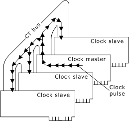
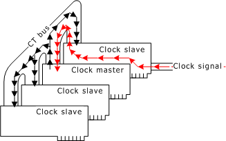
One board on the bus generates (drives) the clock. This board is called the clock master. All other boards use this clock as a timing reference by which they synchronize their own internal clocks. These boards are called clock slaves. The following illustration shows the clock master and clock slaves:

Two CT bus clocks can run simultaneously on the bus. They are called A_CLOCK and B_CLOCK. The clock master can drive either one. When you set up CT bus clocking, choose one of these clocks for your master and slaves. The other one is a redundant signal that can be used by a secondary clock master (described in Secondary clock master fallback).
In the following illustration, the system is set up to use A_CLOCK:
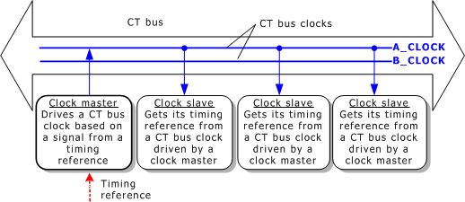
To drive its CT bus clock, a clock master takes a reference signal, extracts the frequency information, defines a phase reference at the extracted frequency, and broadcasts this information as A_CLOCK or B_CLOCK. This reference signal is called a timing reference. When you set up a clock master, you specify what source the board uses as its timing reference.
The timing reference signal originates in one of three places:
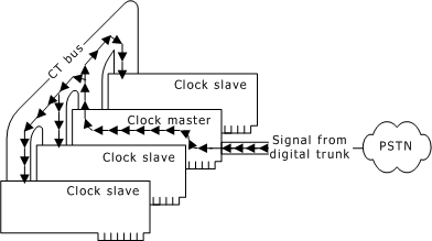
It can originate within the public network and enter the system through a digital trunk. This is called a NETWORK timing reference as shown in the following illustration:
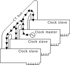
In a system with no digital telephone network interfaces, an on-board oscillator can be used as the timing reference to drive the clock signals. This is called an OSC timing reference and is shown in the following illustration. Use OSC only if there is no external clock source available.
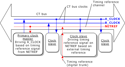
The timing reference used by a clock master to drive the CT bus clock can also originate from an oscillator or trunk connected to another device in the system. In this case, the timing reference signal is carried over the CT bus to the clock master, which derives the clock signal and drives the clock for the slaves. The following illustration shows a timing reference from another device:
The channel over which the timing reference signal is carried to the clock master is called NETREF, as shown in the following illustration:
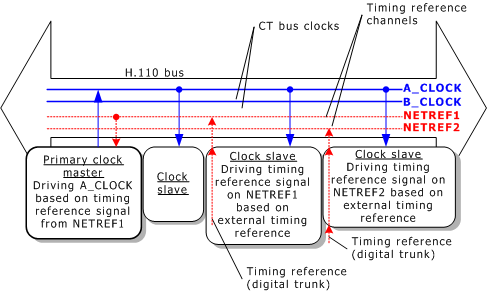
On the H.110 bus, a second timing reference signal can be carried on a fourth channel, called NETREF2 as shown in the following illustration. NETREF is referred to as NETREF1 in this case.
Boards can optionally be assigned a backup (fallback) timing reference that it can use if its primary timing reference fails. For a clock master, the source for the fallback timing reference must be a different source than the one currently used by the clock master for its primary timing reference.
For example, if a clock master's primary timing reference source is a NETWORK signal from one of its trunks, the fallback timing reference source can be a NETWORK signal from another one of its trunks, or a signal from NETREF1, NETREF2 (if H.110), or OSC. In the following illustration, the fallback timing reference source is NETREF1:
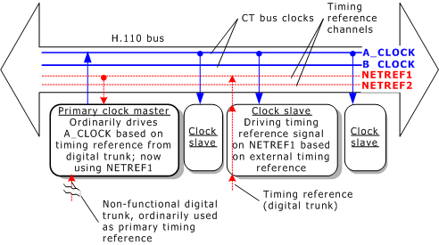
The ability of a board to automatically switch to its fallback timing reference if its primary timing reference fails is called clock fallback. This feature can be enabled or disabled.
The following table summarizes the reference clocks that a clock master can drive:
|
Clock |
Details |
|---|---|
|
A_CLOCK |
The set of primary bit clocks (CT8A) and framing signals (CTFrameA). The CT8A signal is an 8 MHz clocking reference for transferring data over the CT bus. The CTFrameA provides a low going pulse signal every 1024 (8 MHz) clock cycles. |
|
B_CLOCK |
The set of secondary bit clocks (CT8B) and framing signals (CTFrameB). The CT8B signal is an 8 MHz clocking reference for transferring data over the CT bus. The CTFrameB provides a low going pulse signal every 1024 (8 MHz) clock cycles. |
The following table summarizes the timing references that a clock master can use:
|
Timing reference |
Details |
|---|---|
|
NETWORK |
The timing signal from a digital trunk attached to the clock master board. Within the digital trunk interface, an 8 kHz reference is derived from the frequency of the incoming signal. The clock master is frequency-locked to this 8 kHz reference so that the long-term timing of the system matches that of the public telephone network. Note: No timing signal is available from an analog trunk. |
|
NETREF/NETREF1 |
The CTNETREF_1 signal. This signal can be 8 kHz, 1.544 MHz, or 8 MHz. Most boards use only 8 kHz signals. |
|
NETREF2 |
(H.110 only) The CTNETREF_2 signal. This signal can be 8 kHz, 1.544 MHz, or 8 MHz. Most boards use only 8 kHz signals. |
|
OSC |
Clock signal derived from an oscillator on the clock master board. Note: Use this timing reference source only if no network timing references are available. |
A TX board can be configured to perform in any one of the following fallback roles:
The clock fallback role a TX board takes is based on how the main clocking parameters are configured. If no fallback clock is configured, the TX board does not participate in any fallback behavior. For more information, refer to Configuring clocking.
Clock fallback for a primary clock master works as follows:
The primary clock master synchronizes with its primary network timing reference and drives the primary CT bus clock.
If the primary network reference fails, the clock master continues to drive the primary CT bus clock, but switches to the fallback network timing reference as its synchronization source.
If the secondary timing reference fails, the primary clock master stops driving the primary CT bus clock, and falls back to the secondary CT bus clock, which is now driven by the secondary clock master off its fallback timing reference.
If the secondary CT bus clock fails, the board falls back to its internal oscillator and continues to monitor the state of the secondary CT bus clock.
If the secondary CT bus clock is reestablished, the board synchronizes again with the secondary CT bus clock.
You can set up a second device to be used as a backup or a secondary clock master if the primary clock master stops driving its CT bus clock (because both of its timing references failed, or it was hot-swapped out).
Clock fallback for a secondary clock master works as follows:
As long as the primary clock master is driving its CT bus clock, the secondary clock master acts as a slave to the primary clock master. However, the secondary master also drives the CT bus clock not driven by the primary master (for example, B_CLOCK if the primary master is driving A_CLOCK).
If the primary clock master stops driving its CT bus clock, all slaves (including the secondary clock master) lose their primary timing reference.
This failure triggers the secondary master to fall back to its fallback timing reference and continue to drive the secondary CT bus clock from the fallback reference.
This failure also triggers other slaves to fall back to the CT bus clock driven by the secondary clock master.
The secondary master and slaves do not switch back to the primary timing reference automatically if the primary reference is reestablished. Software intervention is required prior to any further clock changes.
If the board formerly used as the primary clock master is still active but is not receiving a primary or fallback timing reference, the board becomes a slave to the clock driven by the secondary master.
If the secondary clock master’s fallback clock reference fails, it switches to an internal oscillator and continues to drive the secondary CT bus clock.
Upon recovery of the fallback clock reference, the secondary clock master synchronizes again with the clock reference and continues to drive the secondary CT bus clock based on the fallback reference.
Clock fallback for a clock slave works as follows:
As long as the primary clock master is driving its CT bus clock, the clock slave uses this clock.
Upon detecting failure of the primary CT bus clock, the clock slave switches to the secondary CT bus clock.
If the secondary CT bus clock fails, the board falls back to its internal oscillator and continues to monitor the state of the secondary CT bus clock.
If the secondary CT bus clock is reestablished, the board synchronizes again with the secondary CT bus clock.
The following illustration shows a sample clock fallback configuration:
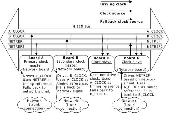
If you specify that any board use NETREF (NETREF1) or NETREF2 as a timing reference, you must configure one or two other boards to drive the signals. Configure a different board for each signal. The source for each signal must be a digital trunk.
Note: NETREF2 is available only in H.110 configurations.
PCI or PCI Express TX boards have a single trunk group consisting of trunks 1, 2, 3, and 4. If the primary or fallback clock reference is a digital trunk, and the board is configured to drive NETREF, the same digital trunk must be configured for both the clocking reference source and the NETREF source. If a different digital trunk is selected for NETREF, this configuration is silently overridden, and the board drives NETREF from the digital trunk selected as the main or fallback clock source.
CompactPCI TX boards have two separate trunk groups. Trunk group one consists of trunks 1, 2, 5, and 6. Trunk group two consists of trunks 3, 4, 7, and 8. If the primary or fallback clock reference is a digital trunk, and the board is configured to drive NETREF, the NETREF source can be either:
The same digital trunk used for the primary or fallback clock reference
Any of the digital trunks in the other trunk group
If a different digital trunk in the same trunk group is selected to drive NETREF, this configuration is silently overridden, and the board drives NETREF from the digital trunk selected as the main or fallback clock source.